|
|
||
Printed Circuit Boards
Printed Circuit Boards (PCB), or Printed Wiring Boards (PWB) as they are sometimes called, have come along way since their invention in 1942 by Dr. Paul Eisler. Originally intended as a replacement for costly cable harnesses they are now found in virtually all electronic equipment.

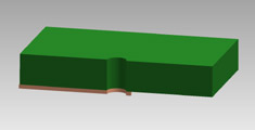
The original boards were simple single sided arrangements. |

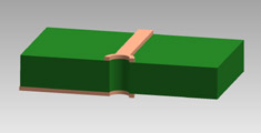
These soon gave way to double-sided boards with the sides connected by pins soldered into holes through the material. |
|
| | ||

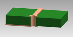
This technique was largely replaced with a thin layer of copper that was plated into the bore of the holes giving rise to the now commonplace Double Sided Plated Through Hole, or DS/PTH, construction. |

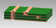
In 1961 the first multilayer boards were produced, where internal layers were sandwiched into the substrate of a Double Sided board. |
As the manufacturing technology improved the number of internal layers were increased and the width of both the tracks and the spacing between these tracks decreased. Further improvements in the tracking density were realised by reducing the size of the holes drilled in the boards and by moving to blind and buried vias which only penetrate those layers necessary to achieve the required connections. By the mid seventies PCBs incorporating 16 layers were being produced, albeit at a high price. In the early eighties the emergence of surface mount techniques drove component densities upward and prompted further size reductions. Line widths and spacing for tracks as small as 0.006" (152 micron) is quite common
Toward the end of the 20th century some advanced manufacturers were beginning to embed low tolerance passive components such as resistors and capacitors within the material of the PCB itself. This technique was developed to allow increased packing densities and reduce costs. Another technique some manufacturers are using is to produce a 3-dimensional circuit on the inside surface of a moulded plastic enclosure. Although this is of limited application, as it is restricted to single sided surface mount usage, it does allow for significant cost savings on simple consumer products where a separate circuit board can be eliminated completely.
It is interesting to reflect on how far PCB technology has come in the short time since its invention. It is also worth noting that the original invention was never patented. If it had been the take up of the technology may have been much slower and early products would have been more costly as a result of royalty costs relating to the patent. Dr. Eisler probably never imagined the universal application of his original idea, and consequently never got rich on his invention.
There are a number of materials used in the construction of PCBs.
Some are for very specialist applications such as the boards that
incorporate an invar metal layer to aid heat dissipation in high-density
power assemblies. Others are flexible circuit boards, and hybrid flex-rigid
boards, that can be folded around the mechanical assembly of their
enclosures. The vast majority are of conventional rigid construction.
The most common substrates are summarized below.
| Type | Construction | Characteristics | Typical uses |
| FR-2 | Phenolic paper laminate | Good electrical and mechanical properties. Corrosion resistance. Low flammability. Good punchability. Low cost. | Entertainment electronics, Automotive. Anywhere that is highly cost sensitive. |
| FR-3 | Epoxy paper laminate. | Similar to FR-2 with improved electrical characteristics. More stable characteristics under unfavourable conditions. | Similar to FR-2 but where improved performance is required without impacting cost. |
| FR-4 | Epoxy glass fibre laminate. | Excellent Electrical & Mechanical properties. Dimensionally stable. Surface qualities. Strength including flexural. Impact resistance. Properties are stable over time and with unfavourable conditions. | The most used option. Professional electronics. Measurement & Control. Aviation. High performance automotive. IT & Communications. Surface mount assemblies. Multi-layer circuits. |
| FR-5 | Epoxy glass fibre laminate | As for FR-4 High temperature use. | As for FR-4 but with a higher temperature requirement. |
| Epoxy aramide paper laminate | Excellent Electrical & Mechanical properties. Strength including flexural. High chemical resistance. Very small thermal expansion coefficients in x, y & z planes. Low dielectric constant & loss. Wide frequency range. | Good at elevated temperatures. Suitable for laser or plasma drilling and routing. Any applications demanding extreme ruggedness or wide temperature ranges. |


